Conducted and Radiated EMI – Practical Troubleshooting Guide
Understanding EMC, EMI, and EMS
- EMC (Electromagnetic Compatibility)
The overall discipline ensuring that electronic devices and systems function properly in their electromagnetic environment without causing or suffering from interference.
EMC = the ability to coexist with other electronics. - EMI (Electromagnetic Interference)
Any unwanted electromagnetic disturbance generated by a device that degrades the performance of nearby equipment.
It can be conducted (through wires or power lines) or radiated (through the air). - EMS (Electromagnetic Susceptibility)
The sensitivity or vulnerability of a device to external electromagnetic fields or conducted noise.
In other words, EMS defines how easily a device is disturbed by EMI.
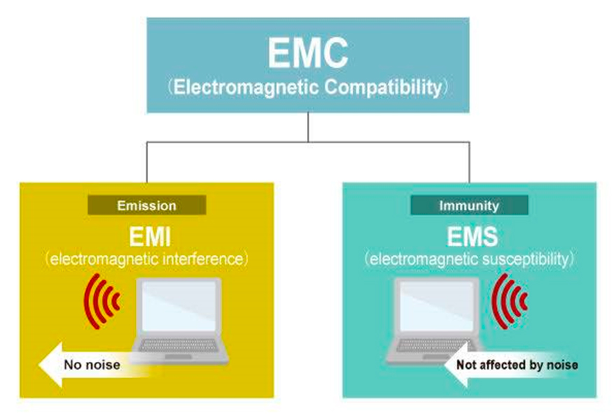
Summary:
- EMC = coexistence goal
- EMI = interference generated
- EMS = interference received
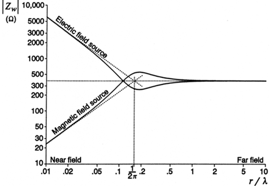
Near and Far Field Regions
In electromagnetic theory, the region around a radiating source is divided into several zones that determine the field characteristics and measurement behavior:
| Region | Approx. Distance from Source | Field Type / Description |
| Reactive Near Field (Fraunhofer) | Typically < λ / (2π) | Strongly coupled electric and magnetic fields; non-radiative energy storage dominates. |
| Radiating (Fresnel) Near Field | Between Reactive Near Field and ~2D²/λ (where D is antenna size) | Partially radiative; used for near-field probe measurements. |
| Far Field | Beyond 2D²/λ | Stable plane-wave region; E and H fields are orthogonal and proportional; used in compliance tests. |
In simpler terms:
- Near-field: Where E and H fields behave independently and are not yet radiated waves (used for PCB-level EMI scanning).
- Far-field: Where emissions propagate as electromagnetic waves, measurable in EMC chambers.

Radiated and Conducted Emissions Troubleshooting Guide
This guide provides a practical, step-by-step workflow for identifying and reducing radiated and conducted electromagnetic emissions during EMC troubleshooting.
It focuses on cost-effective laboratory techniques suitable for pre-compliance evaluation before official certification testing.
Recommended Tools and Materials
Instruments and Equipment
- Near-Field Probe Kit (H-field and E-field):
20 mm H-field probes are standard.
For smaller PCBs, use 10 mm or 5 mm probes to precisely localize emission sources. - Low-Noise or Wideband RF Amplifier (LNA):
Recommended gain: 20–40 dB.
Essential for enhancing probe signal sensitivity. - Spectrum Analyzer:
Choose one with a low noise floor, fine frequency resolution, and fast sweep rate.
Most affordable analyzers are sufficient for pre-compliance testing. - Oscilloscope:
Useful for examining switching waveforms, transient noise, and power integrity. - Differential Voltage Probe (≥ 30 MHz bandwidth):
Optional but effective for separating common-mode and differential-mode noise. - Clamp-On Current Probe (≥ 30 MHz bandwidth):
Optional, used to measure noise currents on power or signal cables.
Materials and Accessories
- Clamp-On Ferrite Beads:
Choose types effective above 30 MHz.
Keep several sizes and shapes for experimentation.
Try multiple cable turns through the core to improve attenuation. - EMI Absorber or Ferrite Sheets:
Non-conductive materials safe for use on PCBs, flat cables, and metal enclosures. - Conductive Fabric Tape (with conductive adhesive):
Excellent for temporary grounding and shielding tests. - Fine Metal Mesh for Cooling Fans:
Openings ≤ 2–3 mm.
A grounded mesh reduces emissions from ventilation areas. - Conductive Fabric or Aluminum Foil:
Handy for temporary or diagnostic shielding experiments. - X- and Y-Capacitors, Multi-Stage AC Line Filters:
Useful for testing filter configurations and improving power-line noise suppression.
Recommended Procedure
Step 1. Pre-Test Scanning in the Laboratory
(Before visiting an EMC test facility)
Radiated EMI Pre-Test (30 MHz – 1 GHz)
Use a 20 mm H-field probe connected to a 20–40 dB LNA and a spectrum analyzer.
These are relative measurements, so DIY or low-cost probes are sufficient.
Safety Note: Check the probe’s isolation voltage rating.
Insufficient isolation can permanently damage the analyzer or LNA inputs.
Inspect these critical areas:
- Switching Regulators:
- Look for ringing or high-frequency spikes.
- Add snubber networks if needed (see TI’s 7-Step Snubber Design Guide).
- Ensure isolated DC/DC converters include Y-capacitors (330 pF – 2.2 nF) between primary and secondary grounds.
- Clock Oscillators and Crystals:
- Verify series termination resistors near clock output pins to reduce overshoot.
- Power Rails:
- Ensure every IC has a local decoupling capacitor close to its VCC pin.
- Long PCB Traces:
- Identify high-speed or unshielded traces acting as antennas.
- Apply EMI absorber or ferrite sheets to reduce radiation.
- Microcontroller GPIOs:
- Reduce drive strength in firmware, particularly for parallel or serial interfaces.
- Cables and Connectors:
- Examine I/O and power interfaces for leakage.
- Check shield continuity at all connectors.
- Add ferrite cores to cables carrying high-frequency noise.
Step 2. EMC Test Facility Troubleshooting
(Locating compliance issues and applying corrective actions)
2.1 Conducted EMI Test (150 kHz – 30 MHz)
Perform a full conducted emissions scan using a LISN and spectrum analyzer.
If the results exceed limits, apply the following countermeasures:
- Add ferrite beads, ring cores, or LC filters on noisy lines.
- Optimize ground return paths and use star-grounding.
- Install common-mode chokes on AC/DC power inputs.
- Shorten power cables where practical.
- Adjust X/Y-capacitor values or add high-inductance cores on power lines.
- If necessary, upgrade the AC line filter (more inductance or multi-stage).
Filter optimization tips:
- Higher common-mode inductance = better suppression.
- Larger X-capacitance = improved differential-mode filtering.
- Y-capacitance is limited in medical-grade equipment for safety reasons.
Finally, use a current probe and oscilloscope to determine which cable carries the main noise current.
Once conducted emissions are within limits, continue with radiated testing.
2.2 Radiated EMI Test (30 MHz – 1 GHz)
Perform a radiated emissions scan in an anechoic or semi-anechoic chamber.
If emissions exceed the limit, apply these mitigations:
- Add snap-on ferrite cores (1–5 turns) to cables.
- Apply EMI absorber or ferrite sheets to noisy PCB zones or flex cables.
- Enhance shielding with conductive fabric or aluminum foil, secured by conductive tape.
- Shorten or reroute cables to minimize coupling and radiating loops.
Step 3. Compliance Verification and Documentation
Once corrective measures have been applied and emissions are reduced, perform a systematic verification to ensure the results are repeatable, stable, and compliant with the intended EMC standard.
3.1 Confirm Emission Margin and Repeatability
- Re-scan the critical frequency bands
- Compare the corrected spectrum with the original baseline.
- Verify at least 3–6 dB margin below the limit line across all relevant bands.
- Watch for narrowband peaks (often from clocks, switching edges) and broadband noise (from switching regulators or digital buses).
- Repeat measurements after system warm-up or mechanical repositioning.
- This ensures the observed margin isn’t due to temporary setup conditions.
- Small changes in cable routing or grounding can alter radiated levels — consistent results prove robustness.
3.2 Documenting Results
Maintain complete traceability and reference for future product revisions or audits.
Essential documentation items:
- Test setup photos (showing cable routing, probe positions, grounding).
- Spectrum analyzer screenshots or CSV exports (before and after mitigation).
- List of applied countermeasures:
- Ferrite types (manufacturer, impedance @ 100 MHz).
- Snubber or filter component values.
- Shielding or absorber materials used.
- Measurement configuration:
- Frequency range, resolution bandwidth (RBW), video bandwidth (VBW), averaging.
- Equipment models.
3.3 Cross-Check With Compliance Limits
Compare results to the applicable standard’s limits:
| Test Type | Frequency Range | Typical Limit Reference |
| Conducted EMI | 150 kHz – 30 MHz | CISPR 32 / EN 55032 Class A or B |
| Radiated EMI | 30 MHz – 1 GHz (and above) | CISPR 32 / FCC Part 15 B |
| Immunity (EMS) | ESD, EFT, Surge, RF | IEC 61000-4-x series |
If all measured levels are comfortably below limits (preferably ≥ 3 dB margin), the design is ready for formal certification.
If not, identify the dominant frequencies and re-apply targeted mitigations (shielding, filtering, layout optimization) before retesting.
3.4 Establish Design Feedback and Prevent Recurrence
- Update the schematic and PCB design guidelines to include successful EMI fixes.
- Create an EMC Design Checklist (e.g., grounding rules, filter placement, cable shield strategy).
- Archive test data and mitigation results for future product variants.
Good EMC design is iterative.
Each prototype and test cycle refines understanding of emission paths, enabling faster compliance in future designs.