Version: 1.1
Author: Elerain
Date: October 2025
-
Introduction
These near-field probes are designed for EMC debugging, EMI localization, and RF field mapping.
The set includes E-field and H-field probes optimized for use with spectrum analyzers, oscilloscopes, or RF receivers up to 3 GHz.
Unlike traditional two-layer probes with exposed copper traces, these probes use a multi-layer PCB structure where all signal conductors are embedded between internal layers, and the probe edges include copper-free safety margins.
This provides enhanced mechanical durability and high-voltage protection during scanning over populated circuit boards or metallic housings.
-
Features
- Multi-layer FR-4 PCB with buried copper for maximum protection.
- Copper-free edges prevent electrical contact with external conductors.
- Slim design allows access between closely spaced components.
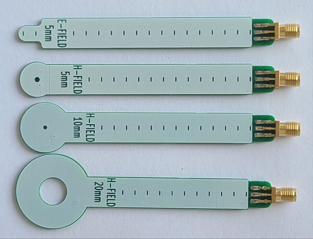
- H-field loop probes in multiple sizes (5 mm, 10 mm, 20 mm).
- E-field probe for electric field detection (5 mm tip).
- Compatible with 50 Ω systems via SMA connectors.
- Suitable for frequencies from 30 kHz to 3 GHz.
- For best performance, use with our 30 dB LNA amplifier to enhance sensitivity.
-
Probe Types and Dimensions
|
Model |
Field Type | Loop/Tap Diameter | Length | Notes |
|
E5 |
Electric Field | 5 mm | 170 mm |
Capacitive tip |
|
H5 |
Magnetic Field | 5 mm | 170 mm |
Fine spatial resolution |
|
H10 |
Magnetic Field | 10 mm | 170 mm |
Medium sensitivity |
| H20 | Magnetic Field | 20 mm | 170 mm |
High sensitivity, lower spatial precision |
-
Electrical Ratings and Protection
Isolation and Safety:
- Copper-to-edge clearance on internal layers: 2 mm
- Dielectric withstand voltage: ≈ 6 kV (transient)
- Continuous working voltage: ≤ 250 Vrms (clean, dry conditions)
- Input impedance: 50 Ω (nominal)
⚠️ Warning:
These probes are designed for low-energy near-field EMI measurements.
Do not contact circuits above 250 Vrms or 400 V DC.
Although the internal copper is shielded, external flashover may occur under high potentials.
⚠️ ATTENTION:
If a near-field probe shows mechanical damage or signs of wear, stop using the probe immediately. Continued use may result in damage to the spectrum analyzer or personal injury.
-
Performance and Frequency Response
- Usable frequency range: 30 kHz – 3 GHz
- Smaller loops provide better localization; larger loops yield stronger coupling.
- E-field probe sensitivity depends on the surface potential gradient.
-
Recommended Setup
- Connect the probe to the spectrum analyzer or receiver using a 50 Ω coaxial cable with SMA connectors.
- (Recommended) Insert a 30 dB LNA amplifier between the probe and your spectrum analyzer to provide signal amplification and additional protection for the analyzer input.
- Adjust the analyzer settings as follows:
- Use a narrow resolution bandwidth (1–100 kHz).
- Enable Max Hold or Trace Averaging as needed.
-
Applications
- Radiated emission troubleshooting
- RF signal tracing in PCB-level diagnostics
- Contactless verification of oscillators or modulators
- EMC pre-compliance screening
-
Technical Summary
|
Parameter |
Specification |
|
Frequency Range |
30 kHz – 3 GHz |
|
Nominal Impedance |
50 Ω |
|
Working Voltage (continuous) |
≤ 250 Vrms / 400 V DC |
| Dielectric Breakdown |
≈ 6 kV (transient) |
| PCB Structure |
Multi-layer FR-4, internal copper |
| Copper-free Edge Clearance |
Present |
| Connector Type |
SMA (female) |
-
Safety Notice
- Avoid probing energized circuits exceeding the rated voltage.
- Do not measure circuits with hazardous potentials.
While the internal copper layers are isolated, accidental flashover from live equipment can still occur, potentially causing damage to the analyzer or personal injury.
Always observe standard ESD and EMC laboratory safety precautions.